

xLight Secures $150M From US Government to Advance Free-Electron Laser Lithography
The United States government has agreed to invest $150 million in xLight Inc., a semiconductor and advanced-laser technology startup developing particle-accelerator-powered Free Electron Lasers (FEL) designed for next-generation chip manufacturing. The investment, offered under a Letter of Intent with the US Department of Commerce, marks one of the most strategically significant CHIPS Act allocations announced this year, positioning xLight at the center of America’s effort to reduce dependence on foreign lithography technologies.
Founded and headquartered in the United States, xLight is focused on building what it calls “the world’s most powerful lasers,” engineering Free-Electron Laser platforms that can be directly applied to semiconductor manufacturing, quantum systems, and national-security-critical photonics infrastructure. The proposed federal investment also signals increasing urgency within Washington to accelerate breakthroughs in foundational semiconductor manufacturing capabilities, especially advanced lithography, where the US currently relies heavily on international suppliers.
Strengthening America’s Position in Advanced Lithography
Lithography remains the single most complex step in semiconductor production, determining transistor scale, wavelength precision, and chip-density ceilings. Today, the most advanced commercial lithography systems come primarily from Europe and Asia, with US fabs depending extensively on external equipment vendors.
xLight’s core proposition is an American-designed and American-manufactured FEL lithography platform capable of achieving photon energy and beam precision beyond current commercial solutions. The company describes its systems as particle-accelerator-driven lasers that generate extremely high-energy photons, unlocking a new category of ultra-short-wavelength lithography suitable for future chip geometries.
With the US seeking to regain semiconductor independence, particularly in high-end foundry processes, the government’s backing signals a strategic shift from simply subsidizing chip factories to actively funding deep-tech capability that underpins fabrication.
First CHIPS R&D Office Award Under the New Administration
xLight reports that the funding commitment is the first award from the CHIPS Research and Development Office (CRDO) under the current US administration. The company says the decision reflects recognition that lithography innovation, not simply fabs, is the key bottleneck now determining global semiconductor competitiveness.
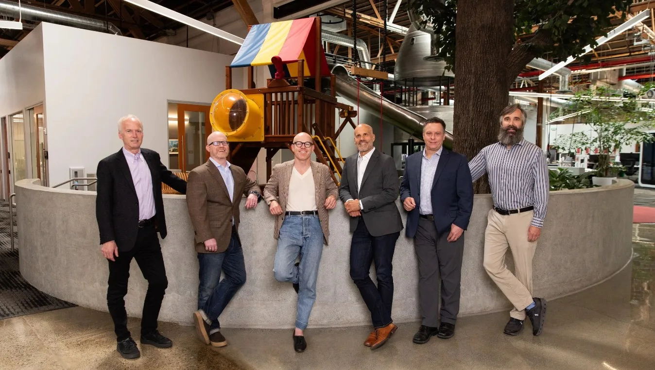
xLight CEO and CTO Nicholas Kelez said the federal backing demonstrated that next-generation lithography has become a core priority. The company will build its first FEL system at the Albany Nanotech Complex, a major semiconductor research facility that hosts multiple global chip development programs and collaborations with leading equipment and manufacturing partners.
Free-Electron Lasers: A New Path for Chip Production
Free-Electron Lasers are traditionally used in physics research and national lab environments due to their extremely high energy and tunability. xLight’s core technology takes accelerator-driven FELs out of laboratory-only use cases and applies them directly to commercial semiconductor workflows. In practical terms, FEL technology could reduce lithography wavelength, enable finer patterning, push past current EUV scaling limits, introduce fully tunable photo-energy sources and accelerate next-generation node migration.
If successful, FEL-based lithography could enable chips beyond the current limits of deep-UV and EUV architectures, something global semiconductor roadmaps increasingly require as physics-driven limitations approach.
A Deep-Tech Team with Scientific and National-Security Focus
xLight brings together particle physics, laser science, semiconductor engineering, and accelerator technology backgrounds, with leadership experience across photonics, national laboratories, accelerator systems, and semiconductor R&D.
Unlike many semiconductor startups focused on software, monitoring, or packaging, xLight is building hard science and high-precision physical infrastructure, a category where investment scale and government collaboration are essential because of the time horizons and national-security dependencies involved. The company openly frames its mission around US national interests, stating its goal is to commercialize FEL systems for “critical economic and national-security applications.”
Why Does This Matters in the 2030 Semiconductor Race ?
The global semiconductor market is now defined by geopolitical strategy as much as commercial competition. The United States has prioritized reshoring chip manufacturing, expanding US-based fabs, and securing advanced semiconductor supply chains across defense, aerospace, communications, and AI compute.
However, even with billions committed to fabs, America remains dependent on global lithography vendors, especially at leading-edge nodes.
With the chip industry entering a phase driven by AI, exascale computing, quantum acceleration, and military systems, the need for secure, domestic photonics capability is intensifying. xLight’s approach seeks to not only advance lithography capability, but anchor that capability inside the US industrial base, a fundamental requirement for sovereignty over next-generation semiconductor tooling.
Strategic Importance: Beyond Funding
Although presented as a funding commitment, this investment represents much more than financial support, it serves as a geopolitical signal that the US intends to compete directly in semiconductor equipment and foundational photonics, rather than relying solely on overseas supply.
It also suggests the CHIPS Act is entering a phase where the government prioritizes capabilities rather than only production capacity, indicating a shift from subsidy-driven policy to technologically targeted investment in enabling infrastructure.
The xLight investment is one of the most strategically meaningful CHIPS Act moves so far, representing a pivot from building fabs to building the core technology those fabs depend on. For decades, advanced lithography has been America’s missing semiconductor piece. If xLight succeeds, it could reshape not only US supply chain resilience but the physics of chip manufacturing itself.
The challenge, however, will not be funding alone but commercialization timelines, scientific complexity, and industrial-scale readiness. While progress remains early, xLight’s FEL roadmap could become one of the most consequential semiconductor bets of this decade.