

How Syenta’s New Approach Could Transform Semiconductor Manufacturing?
The Real Bottleneck in AI Isn’t Compute, It’s Connectivity
The rapid acceleration of artificial intelligence has pushed computing infrastructure into a new phase where the limiting factor is no longer just raw processing power but the ability to move data efficiently between chips, systems, and memory layers, creating a bottleneck that is increasingly difficult to solve using traditional semiconductor design approaches. While advances in GPUs and specialized AI accelerators have delivered significant gains in performance, these gains are often constrained by the physical and architectural limitations of how chips are connected, as data must travel across increasingly complex pathways that introduce latency, consume energy, and reduce overall system efficiency.
This challenge is particularly acute in large-scale AI systems, where thousands of chips must operate in coordination, and where even small inefficiencies in communication can compound into significant performance losses. As a result, the focus of innovation is shifting from individual chips to the systems that connect them, with advanced packaging emerging as a critical area of development that has the potential to redefine how computing hardware is designed and deployed.
Syenta’s Core Idea: Rethinking Chip-to-Chip Communication
Syenta is positioned at the forefront of this shift, developing a new approach to semiconductor packaging that fundamentally changes how chips communicate with each other, enabling higher performance and greater scalability for AI systems. Originating from research at the Australian National University, the company’s technology focuses on advanced chip-to-chip connectivity, addressing the limitations of traditional interconnect methods that struggle to keep up with the demands of modern computing workloads.
By reimagining how chips are packaged and connected, Syenta aims to reduce latency, increase bandwidth, and improve energy efficiency, creating a foundation for systems that can handle the growing complexity of AI applications. This approach reflects a broader trend in the semiconductor industry, where the emphasis is moving away from monolithic chip design toward modular architectures that rely on efficient interconnects to deliver performance gains, and where packaging is becoming as important as the silicon itself.
From Silicon to Systems: The Rise of Advanced Packaging
The significance of Syenta’s work lies in its alignment with a larger transformation within the semiconductor industry, where advanced packaging is emerging as a key enabler of next-generation computing. Traditional semiconductor manufacturing has focused on scaling transistors within a single chip, following the principles of Moore’s Law, but as physical limits are approached, the industry is increasingly turning to packaging technologies that allow multiple chips to be combined into a single system with high-speed connections. This shift toward chiplet-based architectures and heterogeneous integration requires new methods of connecting components in ways that minimize signal loss and maximize performance, and it is in this context that Syenta’s technology becomes particularly relevant.
By providing a more efficient way to link chips together, the company is contributing to a new paradigm in semiconductor design, where performance is achieved not just through smaller transistors but through smarter system integration.
Syenta’s Breakthrough and Its Global Implications
Syenta’s approach has implications that extend beyond individual applications, as it addresses
a fundamental challenge that affects the entire AI ecosystem, from data centers and cloud infrastructure to edge computing and specialized hardware. The ability to improve chip-to-chip communication has a direct impact on the scalability of AI systems, enabling larger models, faster processing, and more efficient use of resources, which in turn supports the continued growth of AI capabilities across industries.
As the demand for AI infrastructure continues to increase, driven by applications ranging from generative models to real-time analytics, the need for solutions that can overcome existing bottlenecks becomes more urgent, positioning companies like Syenta as critical contributors to the next phase of technological development. The company’s global presence, with operations spanning Australia, Europe, and the United States, reflects the international nature of this challenge and the collaborative effort required to address it.

The Emerging Role of Packaging in AI Infrastructure
What distinguishes Syenta’s work is not just its technical innovation but its timing, as it aligns with a moment when the semiconductor industry is actively redefining its priorities in response to the demands of AI. Advanced packaging is no longer a niche area but a central focus of investment and research, as companies recognize that the future of computing depends on the ability to integrate and connect components in more efficient ways. This shift is driving a wave of innovation in areas such as 3D stacking, high-speed interconnects, and system-level design, creating opportunities for new entrants to contribute to the evolution of the industry.
Syenta’s technology fits within this landscape as a solution that addresses one of the most critical aspects of modern computing, providing a pathway to improved performance and scalability that complements advances in chip design and manufacturing.
Syenta Raises $26M to Scale Chip-to-Chip Connectivity for AI
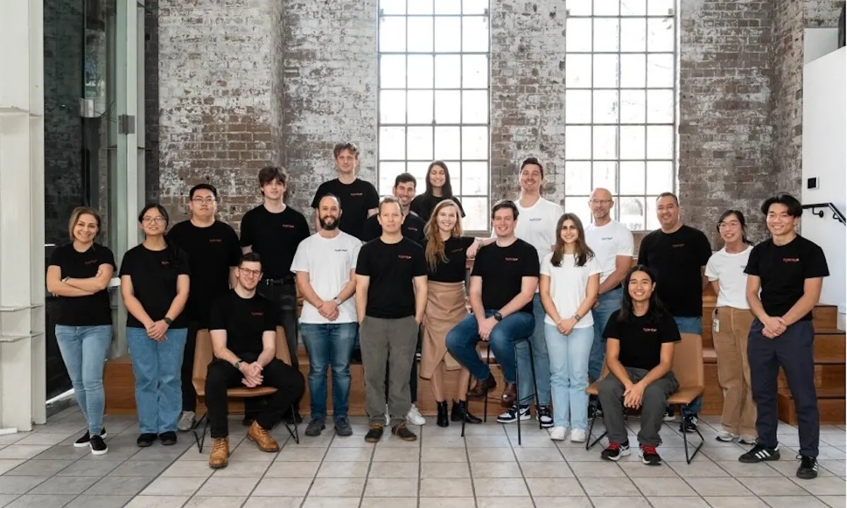
Syenta recently raised $26 million in a Series A funding round, marking a significant step in its journey from research-driven innovation to commercial deployment, as the company looks to scale its advanced semiconductor packaging technology and bring its chip-to-chip connectivity solutions to the broader AI infrastructure market.
The funding reflects growing investor confidence in the idea that the next wave of performance gains in AI computing will come not just from more powerful chips, but from more efficient ways of connecting them, and positions Syenta to accelerate product development, expand its engineering capabilities, and deepen its engagement with global semiconductor and data center ecosystems.
As AI workloads continue to scale in both size and complexity, the demand for high-bandwidth, low-latency interconnect solutions is becoming increasingly urgent, and this investment signals that Syenta is emerging as a key player in addressing one of the most critical bottlenecks in modern computing infrastructure.
The Future of Semiconductor Manufacturing: Beyond the Chip
The broader significance of Syenta’s approach lies in its potential to reshape how semiconductor manufacturing is conceptualized, moving beyond a focus on individual chips to a systems-oriented perspective where the interactions between components are as important as the components themselves. As AI continues to drive demand for more powerful and efficient computing infrastructure, the ability to design systems that can operate at scale without being constrained by communication bottlenecks will become increasingly important, and this is where innovations in packaging and connectivity will play a decisive role.
Syenta represents a new generation of semiconductor companies that are not just building better chips but redefining the architecture of computing systems, and while the path to widespread adoption will depend on factors such as industry standards, partnerships, and manufacturing capabilities, the direction it represents is clear: the future of computing will be shaped as much by how chips are connected as by how they are built.