

Indian Scientists Demonstrate 100 Gbps Silicon Photonic Chip for 6G Technology
JNCASR-led Scientists demonstrates photonic Klein tunnelling in silicon-based terahertz circuits, opening new possibilities for high-speed 6G communication hardware.
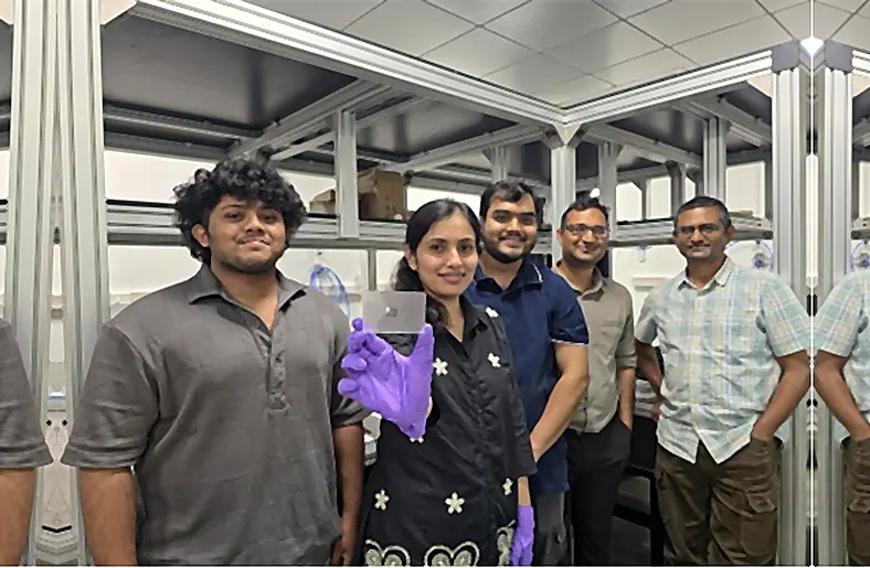
Indian researchers have experimentally demonstrated a silicon-based photonic chip capable of supporting data transmission rates of up to 100 gigabits per second (Gbps), marking a significant development in terahertz communication research for future 6G networks. The research, conducted at the Jawaharlal Nehru Centre for Advanced Scientific Research (JNCASR), Bengaluru, demonstrates a technique that allows terahertz signals to pass through engineered barriers within a photonic circuit with minimal disruption.
The study, titled Photonic Klein Tunnelling in Silicon Topological Materials for Terahertz 6G Interconnects, was published in the journal Advanced Materials on October 11, 2026. The research was led by Abhishek Kumar of JNCASR, with Samina Mulla and Sangram Kumar Sadhu as joint first authors. The collaboration also involved researchers from the Indian Institute of Science Education and Research (IISER) Kolkata, IIT Bombay, Singapore’s A*STAR Institute of Microelectronics and research institutions in France.
At the centre of the research is a silicon valley photonic crystal, a specially engineered structure that controls the movement of electromagnetic waves. The researchers fabricated a silicon slab containing a repeating arrangement of tiny triangular holes. By carefully adjusting their geometry, they created pathways through which terahertz signals could travel. The design is compatible with Complementary Metal-Oxide-Semiconductor (CMOS) technology, an established platform used in semiconductor manufacturing.
The key scientific principle behind the demonstration is known as photonic Klein tunnelling. The concept draws on Klein tunnelling, a phenomenon first studied by physicist Oskar Klein in 1929 in the context of relativistic quantum particles encountering potential barriers. In this experiment, researchers demonstrated an analogous effect in a photonic system. They introduced engineered barriers into a valley-based waveguide channel and investigated how terahertz signals behaved when crossing them. Unlike conventional wave propagation, where barriers can cause reflection and scattering, the specially designed structure allowed transmission to remain close to its barrier-free level under specific conditions.
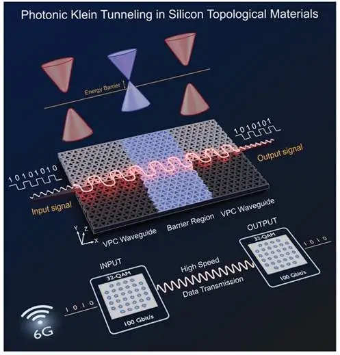
The researchers found that signal transmission remained largely unaffected when the engineered barrier strength was below a particular coupling threshold. Transmission was strongly suppressed as the barrier strength approached that threshold. Momentum-space analysis also showed that valley pseudospin was preserved with greater than 98 per cent fidelity across two consecutive barriers, indicating that the engineered propagation characteristics were maintained.
To demonstrate the practical capabilities of the approach, the team developed three device configurations: a multibarrier structure, an omega-shaped waveguide and a power splitter. These devices demonstrated Klein-tunnelling-based terahertz transport, supporting data transmission rates of up to 100 Gbps. The power-splitter configuration achieved the highest reported rate. The findings establish an experimental basis for using this approach in high-capacity terahertz photonic integrated circuits.
The research is relevant to 6G development because terahertz frequencies are being investigated for future wireless communication systems that require greater bandwidth and data-carrying capacity. However, handling signals at these frequencies presents challenges, including efficient signal generation, transmission, detection and routing. The JNCASR team’s work addresses the signal-routing aspect by demonstrating controlled terahertz propagation across engineered barriers in a silicon photonic structure.
The researchers identify further work on electrically, thermally and mechanically controlled barriers as a possible direction for future investigation. Such control could enable reconfigurable photonic circuits with dynamically adjustable signal pathways.
The demonstration does not represent a complete 6G communication system or a commercially available 100 Gbps chip. However, it provides an experimentally demonstrated approach to managing terahertz signals within CMOS-compatible silicon photonic structures, an important area of research for future high-speed communication hardware.